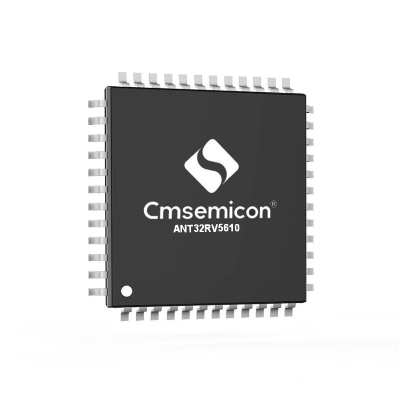
ANT32RV56xx has built-in 2 operational amplifiers and 2 comparators, 2 programmable gain amplifiers, which can replace off-chip operational amplifiers and comparators for wireless charging and decoding circuits. It can quickly provide effective protection against abnormal situations in system control. The chip has two built-in high-precision 12-bit ADCs, low-speed and high-speed, which can accurately collect voltage, current and temperature signals for system control for different application scenarios; The flexible configuration of enhanced PWM is suitable for half-bridge and full-bridge control, and the fast braking function can effectively protect the entire control system.
> RISC-V core 48MHz@2.1V~5.5V
-RV32EC instruction architecture
> Memory
-64KB Flash, 1KB Data Flash, 32KB ILM-SRAM, 8KB DLM-SRAM
-Support BOOT function, space can be set to 0~4KB
> Flexible configuration The system clock can be switched freely
-Internal high-speed RC oscillation: 48MHz
-Internal low-speed oscillation: 40KHz
> Abundant timers
-1 24-bit timer
-4 32-bit/16-bit optional general-purpose timers
-1 32-bit watchdog timer
-1 6-bit window watchdog timer
> 32-bit hardware divider
-with unsigned mode, 6 clock cycles completed
> built-in high-precision temperature sensor
> dedicated PWM module for motor control
-Support independent/complementary/synchronous/group output mode
- Support center symmetrical and asymmetrical mode
- Support single/continuous/interval loading mode
- PWM port line with remapping function
- Any edge or period of PWM can trigger ADC conversion
- Support Wave-by-wave current limiting PWM function
> High-precision 12-bit ADC-Built
-in 1 low-speed 12-bit ADC@100Ksps-Built
-in 1 high-speed 12-bit ADC@1.2Msps
-Both low-speed and high-speed ADCs use 12 external channels, 8 Internal channel architecture
-Each channel has an independent result register
> Abundant analog peripherals
-Built-in 2 high-performance operational amplifiers (10MHz, 10V/us)
-Built-in 2 high-performance analog comparators, support bilateral hysteresis function (10mV /20mV/60mV)
-Built-in 2 PGA, 4~32 times gain optional
> Support general cyclic redundancy check unit (CRC)


 8-bit microcontroller
  32-bit microcontroller
  RISC-V
  High performance and low power consumption
  Brushless DC motors
  High precision measurement
  Wireless connection
  Electromagnetic heating
  Automotive MCUs
  High precision ADC
  Touch
Touch  Display driver
  IPM driver
  Gate driver
  Motor driver
  Auto Body System
  Motor System
  Smart office
  White goods
  Digital power supply
  Personal care
  green riding
  Garden tools
  Electric tools
  Fan water pump
  Kitchen appliances
  Lithium battery management
  Family medical
  Personal medical
  CCC
CCC  Personal care


